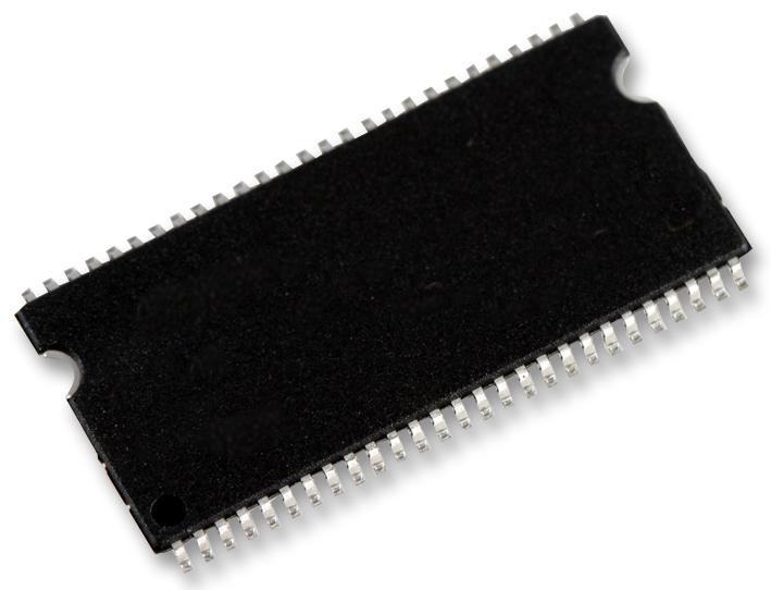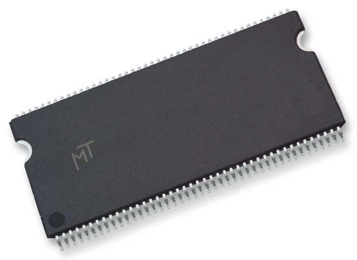
ALLIANCE MEMORY AS4C64M8D2-25BIN DRAM, DDR2, 512 Mbit, 64M x 8bit, 400 MHz, FBGA, 60 Pins
Product Overview
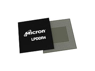
AS4C64M8D2-25BIN is a 512M � (64M x 8bit) DDRII synchronous DRAM (SDRAM). The 512Mb DDR2 SDRAM is a high-speed CMOS double-data-rate-two (DDR2), synchronous dynamic random-access memory (SDRAM) containing 512Mbits in an 8-bit wide data I/Os. It is internally configured as a quad bank DRAM, 4 banks x 16Mb addresses x 8 I/Os. The device is designed to comply with DDR2 DRAM key features such as posted CAS# with additive latency, write latency = read latency -1, and on-die termination (ODT). All of the control and address inputs are synchronized with a pair of externally supplied differential clocks. Inputs are latched at the cross point of differential clocks (CK rising and CK# falling). All I/Os are synchronized with a pair of bidirectional strobes (DQS and DQS#) in a source synchronous fashion. The address bus is used to convey row, column, and bank address information in RAS #, CAS# multiplexing style.
- JEDEC standard compliant, supports JEDEC clock jitter specification
- Fully synchronous operation, fast clock rate: 400MHz, differential clock, CK and CK#
- Bidirectional single/differential data strobe, 4 internal banks for concurrent operation
- 4-bit prefetch architecture, internal pipeline architecture, precharge and active power down
- Programmable mode and extended mode registers, posted CAS# additive latency (AL): 0, 1, 2, 3, 4, 5
- WRITE latency = READ latency - 1 tCK, burst lengths: 4 or 8 burst type: sequential/interleave
- DLL enable/disable, on-die termination (ODT)
- Auto refresh and self refresh, 8192 refresh cycles/64ms
- 60 ball FBGA package
- Industrial temperature range from -40°C to 95°C
Product details
Other details
| Brand | ALLIANCE MEMORY |
| Part Number | AS4C64M8D2-25BIN |
| Quantity | Each |
| Technical Data Sheet EN |
All product and company names are trademarks™ or registered® trademarks of their respective holders. Use of them does not imply any affiliation with or endorsement by them.
ALLIANCE MEMORY AS4C64M8D2-25BIN DRAM, DDR2, 512 Mbit, 64M x 8bit, 400 MHz, FBGA, 60 Pins
Product Overview
AS4C64M8D2-25BIN is a 512M � (64M x 8bit) DDRII synchronous DRAM (SDRAM). The 512Mb DDR2 SDRAM is a high-speed CMOS double-data-rate-two (DDR2), synchronous dynamic random-access memory (SDRAM) containing 512Mbits in an 8-bit wide data I/Os. It is internally configured as a quad bank DRAM, 4 banks x 16Mb addresses x 8 I/Os. The device is designed to comply with DDR2 DRAM key features such as posted CAS# with additive latency, write latency = read latency -1, and on-die termination (ODT). All of the control and address inputs are synchronized with a pair of externally supplied differential clocks. Inputs are latched at the cross point of differential clocks (CK rising and CK# falling). All I/Os are synchronized with a pair of bidirectional strobes (DQS and DQS#) in a source synchronous fashion. The address bus is used to convey row, column, and bank address information in RAS #, CAS# multiplexing style.
- JEDEC standard compliant, supports JEDEC clock jitter specification
- Fully synchronous operation, fast clock rate: 400MHz, differential clock, CK and CK#
- Bidirectional single/differential data strobe, 4 internal banks for concurrent operation
- 4-bit prefetch architecture, internal pipeline architecture, precharge and active power down
- Programmable mode and extended mode registers, posted CAS# additive latency (AL): 0, 1, 2, 3, 4, 5
- WRITE latency = READ latency - 1 tCK, burst lengths: 4 or 8 burst type: sequential/interleave
- DLL enable/disable, on-die termination (ODT)
- Auto refresh and self refresh, 8192 refresh cycles/64ms
- 60 ball FBGA package
- Industrial temperature range from -40°C to 95°C
Product details
Other details
| Brand | ALLIANCE MEMORY |
| Part Number | AS4C64M8D2-25BIN |
| Quantity | Each |
| Technical Data Sheet EN |
All product and company names are trademarks™ or registered® trademarks of their respective holders. Use of them does not imply any affiliation with or endorsement by them.
Product Information
Product Information
Shipping & Returns
Shipping & Returns
Description
Product Overview
AS4C64M8D2-25BIN is a 512M � (64M x 8bit) DDRII synchronous DRAM (SDRAM). The 512Mb DDR2 SDRAM is a high-speed CMOS double-data-rate-two (DDR2), synchronous dynamic random-access memory (SDRAM) containing 512Mbits in an 8-bit wide data I/Os. It is internally configured as a quad bank DRAM, 4 banks x 16Mb addresses x 8 I/Os. The device is designed to comply with DDR2 DRAM key features such as posted CAS# with additive latency, write latency = read latency -1, and on-die termination (ODT). All of the control and address inputs are synchronized with a pair of externally supplied differential clocks. Inputs are latched at the cross point of differential clocks (CK rising and CK# falling). All I/Os are synchronized with a pair of bidirectional strobes (DQS and DQS#) in a source synchronous fashion. The address bus is used to convey row, column, and bank address information in RAS #, CAS# multiplexing style.
- JEDEC standard compliant, supports JEDEC clock jitter specification
- Fully synchronous operation, fast clock rate: 400MHz, differential clock, CK and CK#
- Bidirectional single/differential data strobe, 4 internal banks for concurrent operation
- 4-bit prefetch architecture, internal pipeline architecture, precharge and active power down
- Programmable mode and extended mode registers, posted CAS# additive latency (AL): 0, 1, 2, 3, 4, 5
- WRITE latency = READ latency - 1 tCK, burst lengths: 4 or 8 burst type: sequential/interleave
- DLL enable/disable, on-die termination (ODT)
- Auto refresh and self refresh, 8192 refresh cycles/64ms
- 60 ball FBGA package
- Industrial temperature range from -40°C to 95°C
Product details
Other details
| Brand | ALLIANCE MEMORY |
| Part Number | AS4C64M8D2-25BIN |
| Quantity | Each |
| Technical Data Sheet EN |
All product and company names are trademarks™ or registered® trademarks of their respective holders. Use of them does not imply any affiliation with or endorsement by them.